Name that Ware, July 2026

July 30th, 2026

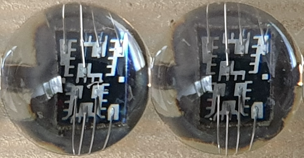
The Ware for July 2026 is shown below.

I’ve got silicon on the brain, so I’m going to give a die shot another go at name that ware. Hopefully this one is a bit easier than the last one. This excerpt is a design pattern I look for and find on almost every SoC. It’s technically showing a bit more than just the part I’m focused on, so as a hint I’m primarily interested in identifying the structure towards the lower left corner of this image.

If you’ve seen one of these before, you’ll know what it is – it’s pretty unmistakable, and a design pattern that’s highly conserved across processes, nodes and foundries. Bonus points to anyone that can explain some of the reasons why things are organized the way they are!

Winner, Name that Ware June 2026

July 30th, 2026

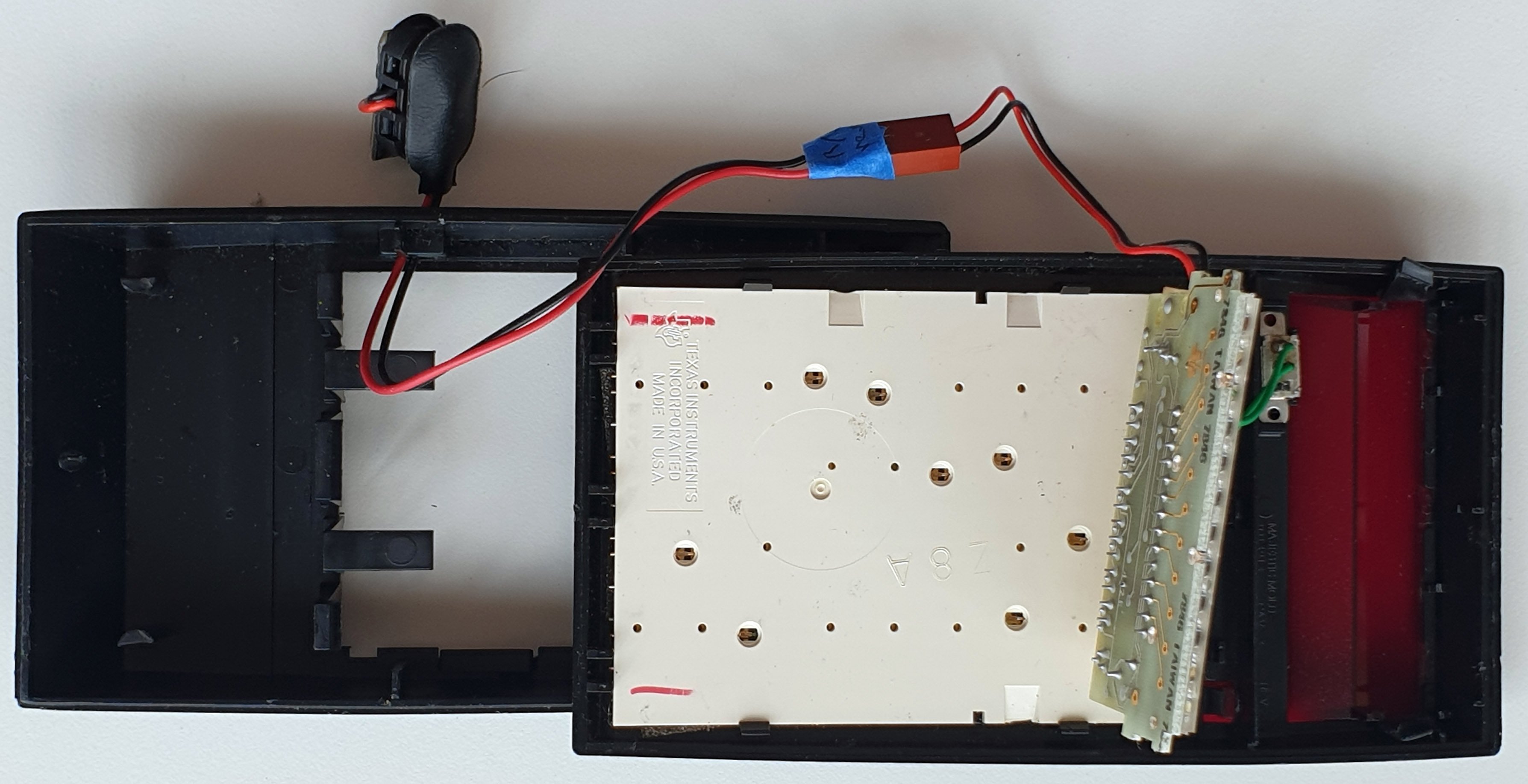
The Ware for June 2026 is an SGI RM6-64 raster manager, from a KONA/InfiniteReality graphics system. Congrats to Christian for naming it! email me for your prize.

This gem of a board was gifted to me by someone at SGI back when I worked there in…I want to say 1998? I even still have the name plate from my cubicle, from back before the ‘bunnie’ nickname really stuck…

Back then, if you wanted to do graphics, SGI was the only game in town, but I joined the party late. Within six months of joining, most of the division I was in had jumped ship for these then little-known upstarts of nVidia and ATI. Lacking any connections and the office a ghost town (my office building was eventually acquired by another startup that’s become a household name, you might have heard of them: Google. Still really weird visiting friends that work on that campus…), I went back to the familiarity of MIT and got my PhD, and that was the last time I held a job in Silicon Valley. Ironically, my main project today is doing silicon, just not in the Valley. What’s that old saying…you can take the boy out of Silicon Valley, but you can’t take the silicon out of the boy?

It was pretty impressive what they could do at the board level at SGI. That all got eaten up by Moore’s Law and integrated graphics…and now that Moore’s Law has run out of steam, we’re returning with gusto to the huge rack servers with lots and lots of interconnect!

Name that Ware, June 2026

June 30th, 2026

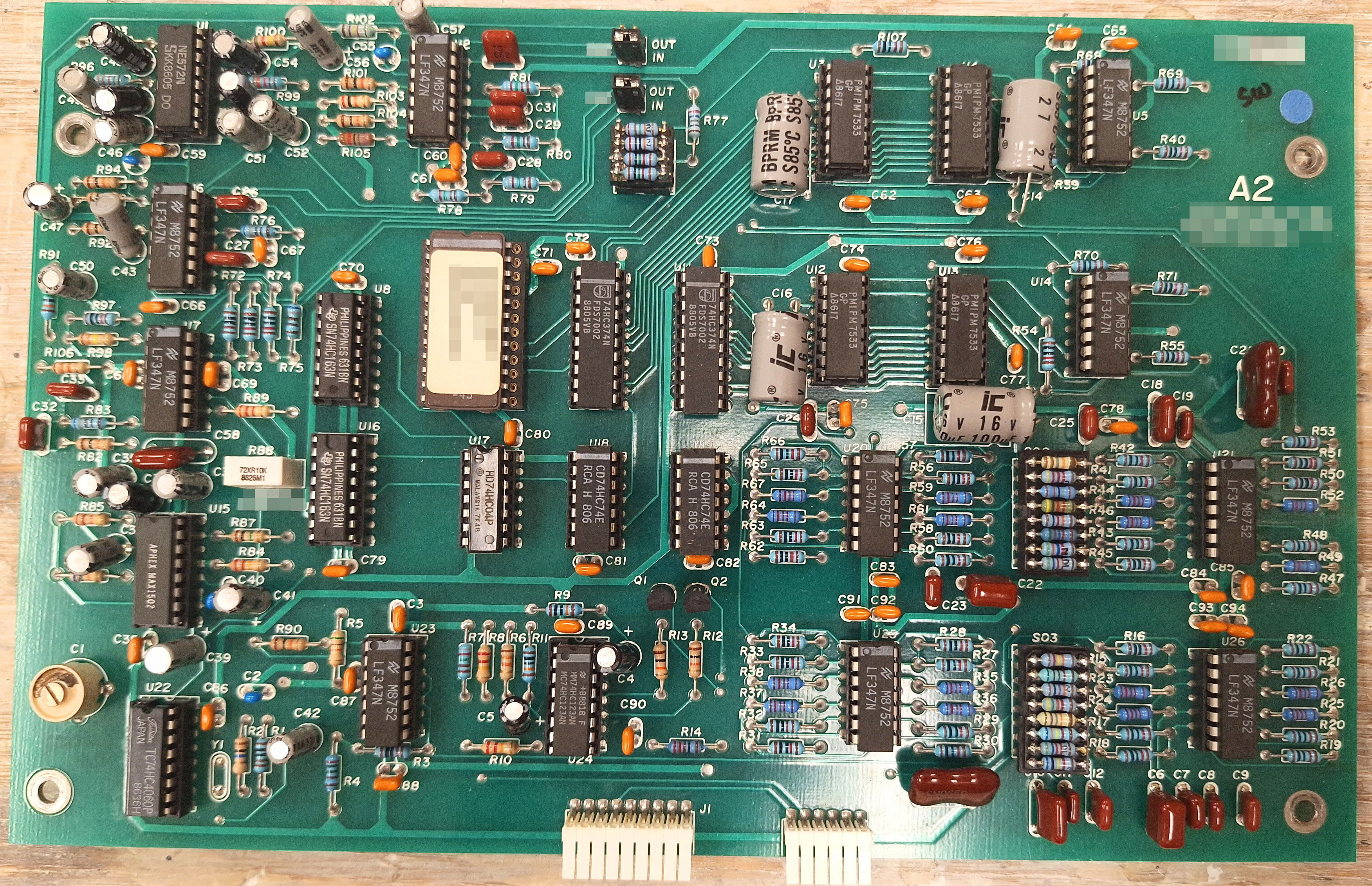
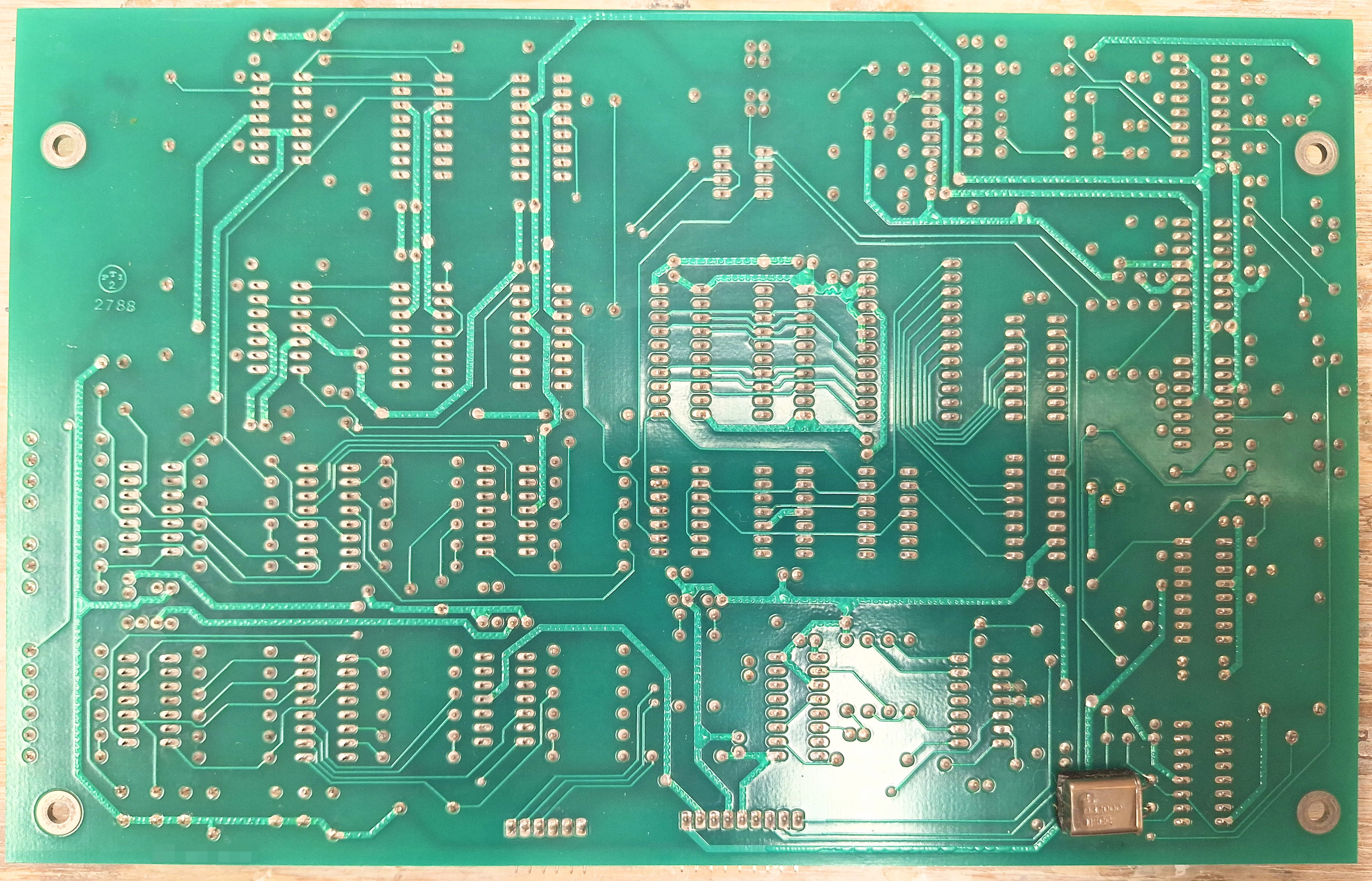
The Ware for June 2026 is shown below:

This board is from my personal collection of “favorite boards” that I’ve collected over the years. A lot of old memories associated this one – both figuratively and literally.

I’ve received some feedback that gmail in particular is marking my email updates as spam. Not sure I have a good way to fix this yet, as the blog is also under heavy attack from automated AI spammers at the same time (to the tune of several thousand requests a day).

You’ll notice that the blog has no ads, so I also have no budget for moderation, paid mailers, or fancy anti-spam tools. I’ll noodle on a durable solution to this problem in my copious spare time, but for now, if you’re not receiving the email updates, please try to convince Google this is not spam by marking it as ham in your inbox. Yes, have also received feedback that this is ineffective and that “the way” is to pay a service that specializes in sending spam *ahem* marketing emails, but see my previous comment about this being a lean, ad-free blog. But, maybe if enough readers mark the emails as not spam, “The Algorithm” might be convinced people actually wanted the updates they signed up for?

Solution, Name that Ware May 2026

June 30th, 2026

The Ware for May 2026 is, in FETguy’s words: “one of many large pc boards of a Rodgers Instrument Co church organ. The core memory was used to store and recall settings of the organ’s “stops”. There were 5 core memory boards in this instrument which differ in how many words were implemented. I photographed the largest one, which has 19 x 10 bit words, of which one is a spare, and then another word, I guess also spare, with no corresponding drive circuitry populated. So, 200 cores of which 180 were actually used.”

Here’s the unredacted version of the ware – includes a patent number which has more details about how it works. I love the design-for-repair, self-documenting nature of this board!

Nobody quite guessed the true nature of the ware, so this month there’s just a solution and no prize.

On Reading SRAMs in IR Images, and Establishing Bounds on Trust

May 31st, 2026

Last month’s name that ware demonstrates that even though non-destructive IR imaging is not capable of resolving an individual bit cell, at least at 22nm it is still possible to constrain the number of bits in an SRAM macro.

An important step in establishing trust in a computer is measuring all of its state and confirming that nothing is amiss. A typical trusted boot would make a point of zeroing and/or patterning & hashing all the known bits of memory in a system. This process helps constrain the amount of malicious or foreign code that could be hiding in the system.

Physical measurements are important is because it’s possible for designers to “hide” memory from this check. For example, inserting a few kilobytes of RAM into a chip the size of the Baochip-1x would not affect the die size. Likewise, its impact on power consumption would be indistinguishable from offsets due to normal manufacturing tolerances. Furthermore, the presence of the RAM can be masked from a pure software inspection by gating it off using a “secret knock” register that only activates the memory when challenged with a correct sequence of words. This makes it practically impossible to discover hidden memories with a brute force address space scan. Such a memory would evade security measurements, and thus makes a useful primitive for staging malicious operations.

IR imaging can place an upper bound on how much SRAM is on a chip. This allows end users to check that all the RAM claimed to be in an open-RTL system (such as the Baochip-1x) matches what was actually fabricated. This in turn puts strong bounds on certain security operations, such as zeroing and/or measuring the state of all known RAM bits in a system.

The good news is that a simple physical measurement through IR inspection thoroughly eliminates the possibility of extra RAM macros in a system, as such a block would be observable even by the most entry-level home IRIS setup: the smallest blocks of RAM are gigantic compared to the resolution of an IR scan. The number of claimed blocks should strictly line up with the number shown in the source code, as it does in the case of the Baochip-1x.

That being said, it’s worth asking if an attacker could “just make a few bytes of RAM in a subtle way” or perhaps “just insert an extra row or column” in an existing macro. To understand the answer to this question better, let’s take a look at deeper look at the structure of an SRAM macro.

How to Read SRAM Macros

Above shows some details on the “rdram1kx32” RAM macro (“Macro D” from the competition) that makes up the data cache elements for the RV32 in the Baochip-1x. From the source code, we can see that this is a dual-port (1r/1w) RAM, organized as 1024 x 32 bits. I’ve rotated the RAM macro so that it’s in canonical “textbook” orientation, such that the columns go vertically and the rows go horizontally. When looking at a micrograph like this, generally speaking, lighter areas are metal-heavy, and darker areas are transistor-heavy. The transistor-heavy RAM arrays correspond to the eight dark rectangles on either side of a central spine.

Such a central spine is a common motif in circuit design. Splitting circuits in half reduces the maximum wire length by half, compared to sticking all the drive circuits on one side. Circuits work equally well when laid out in mirror-image, thus allowing techniques like this to achieve perfect symmetry around a central axis.

I’ve labeled some of the macroscopic features of the RAM. Along the center of the macro, you can see two banks of address decoders. You can use this structure as a “tell” for whether you’re looking at a single or dual port RAM macro. The bottom edge has the column sense amps & drivers. Each column shares circuitry across 4 bits, so their pitch is quite wide and thus visible even at IR wavelengths. Here you can readily count the number of bits in each half of the macro, 16 on each side, giving us a total of 32 bits.

The RAM is further subdivided into four distinct black rows on either side, with some sort of stippled “metal-heavy” region stitched in between. These stippled regions are inserted into RAM macros to improve their performance – they are repeaters that reduce the maximum length of a wire between RAM cells and their corresponding drivers. Repeaters are essential for performance because the wires in a RAM array are minimum-width for maximum density. This means they are quite resistive – in fact, they behave closer to a chain of resistors than ideal wires. Thus, higher performance can be achieved by reducing the wire length through the insertion of repeaters like this.

This leaves us now looking at the RAM array itself. The actual storage cells are too small to see, but we can infer that its size must be 256 bits x 16 bits total gross storage. The actual organization is (4×64)x16 bits – in other words, each of those column circuits is connected to 4 bits of memory, and the lower two bits of address are used to select between those, while 6 bits of address are decoded to select between 64 rows inside that gray blob.

Above is detail of the bioram1kx32 macro (“Macro A“). From the RTL, we can infer that this is a single-port, 1kx32 RAM. Here, you can see the central spine consisting of the single-port address decoder, and then on the lower edge mirror-symmetric 2×16 bit data in/out drivers/sense amps. Again, the core memory cells are laid out in a (64×4)x16 pattern, but in this case, we don’t have any repeaters between the banks. The single-port structure required of the BIO means we can hit the necessary timing without losing density to repeaters. Of course, we pay for this in the lower IPC of the BIO (due to separate read and write phases to the RAM), but for this design, a primary concern was keeping the cores small, so it works out.

And finally, above, here’s some detail of the aoram1kx36 RAM macro (“Macro E“). This has a structure distinct from the previous two: this is a density-optimized RAM macro. Here the address decoders occupy the yellow “spine” down the middle, and the column drivers/decoders are also primarily along the middle instead of along the edge. We can just barely make out the number of columns, and we have to infer that the rows are 512 deep organized as 128×4. While the merits of the density-optimized macro doesn’t really shine for such a small chunk of RAM, I’ll leave it as an exercise to the reader to look at the ifram32kx36 macro and observe how the structure scales up favorably compared to the smaller performance-oriented macros.

One side note is that in a modern silicon process, RAM macros are always in the same orientation across the entire chip. There are increasingly strict rules on the orientation of transistor gates as node size diminishes – fabs hyper-optimize yield for a single orientation and spacing of transistor gate relative to the crystalline lattice of the base silicon. Transistor gates are not so much as “drawn”, but carved out of sub-wavelength interference patterns. For some fairly solid technical reasons, you never have to worry about looking for RAMs built at funny angles or orientations.

No Place to Hide?

Now that we understand a little more about the structure of the RAM macros, let’s return to the question of places where we could hide “a little bit” of extra memory.

First, let’s observe that every SRAM bit is accompanied by some overhead circuitry. For various circuit-level reasons, it’s not possible to “just” lay down some extra-tiny SRAM cells without the supporting decoder, amplifier and driver circuitry. Thus, even the smallest “extra” RAM macro would be noticeable, if not simply for the presence of all the overhead circuitry surrounding the SRAM.

We can also observe that in all cases, we’re able to clearly see the number of columns in an SRAM. Thus, widening an SRAM by adding bits to its datapath would be clearly evidenced by the additional column drivers.

The tricky case is extra rows. We definitely can’t make out individual rows – we can only infer their existence by the process of eliminating the observed datapath widths against the list of possible RAMs on the chip. Here we need to make a distinction between attackers that can only generate fab-approved RAMs, versus an attacker that can modify RAM arbitrarily. RAMs are some of the densest, most difficult to fabricate structures, so in general fabs would not accept a design with true custom RAM.

In the case that an attacker is someone working at the netlist level and trying to insert a trojan in the RTL, I would argue this would be detectable because “just adding another row” of memory has ripple effects onto the memory organization. For example, a 1024×32 RAM already has all the row decoders fully-occupied. Building a 1028×32 RAM (recall that the rows come in increments of 4 bits) would add an extra level to the address decoders and a noticeable offset to the row size.

In the case that an attacker is someone with the necessary fab privileges to make small, customized modifications to the RAM macro, I would say it’s a coin toss if it can be detected with an IR level scan: definitely detectable in an older node, and probably detectable in 22 nm. The extra row will need space, and you’d need some circuitry to handle hiding it; but I can’t definitively rule out that someone can’t be clever enough to make it so small that it’s within the noise margin of an IR inspection. That being said, RAM cells are not infinitesimally small, and further measurements with e.g. laser interferometry could characterize sub-wavelength interference patterns with coherent light to detect even subtle changes in highly regular arrays such as SRAMs. In any case, a destructive inspection tool such as SEM can be used to follow up on any suspect structures and find ground truth.

That being said, a full custom RAM macro is a lot of work for just a single row of memory. While a row of RAM is enough to perhaps hide a shadow copy of a cryptographic key, one would still need to consider where the code or logic would be hidden that both obscures the extra row’s existence from an address space scan, and also choreographs the attack in a useful fashion.

While it’s somewhat unsatisfying to conclude that we can’t rule out every conceivable attack with simple visual inspection, I take solace in the fact that the majority of the attack surface is ruled out, and we now know what sorts of measurements and attacks are relevant to focus on from a defense perspective.

The types of attacks that are possible with and without visual inspection of the chip are vastly different. Without inspection, an attacker is readily able to hide several kilobytes of RAM behind a secret knock; with inspection, we’re looking for at most a few dozen bytes of RAM in an otherwise unprotected array. We turn an effectively unbounded search for hidden memory into a much more tractable proof-of-space measurement, with a caveat that it’s possible for a few extra bytes to be hidden by a determined adversary. I feel that this caveat is diminishingly small, as these extra bytes are very expensive to inject, yet still readily detectable with other means, tilting the cost/reward function towards “not worth it” on the list of potential attacks an adversary could spend resources on.

You Can Try It at Home!

In addition to the practical application of security measurements, I think it’s just interesting to be able to look at a piece of silicon and determine how much RAM is located where. I’m always curious about what makes things tick, and this is yet another tool in the toolbox that allows me to peer through the veil and see into the heart of my hardware. In the spirit of name that ware, I hope this spurs more people to look at silicon, and to learn what we can by observing the design patterns harbored within our gadgets. If you want to learn more about using IR to read CSP-packaged chips such as the Baochip-1x, check out my IRIS page, or just skip to a video I made on how to modify an off the shelf USB camera microscope into an IR camera.